Belghachi, A. and N. Limam, 2017. Effect of the absorber layer band-gap on CIGS solar cell. Chinese J. Phys., 55(4): 1127-1134.
Research Journal of Applied Sciences, Engineering and Technology
Optimization of the Electrical Characteristics of Cadmium Telluride Based Thin Layer Solar Cell According to Thickness and Gap Energy
Research Journal of Applied Sciences, Engineering and Technology 2020 17: 129-135
Cite This ArticleAbstract
In the quest for better photovoltaic performance, we simulated the CdTe-based thin film solar cell in ITO/CdS/CdTe/Mo structure with SCAPS (Solar Cell Capacitance Simulator). SCAPS model makes possible to study the effect of the thickness of layers and the gap energy (Eg) of each layer (CdTe, CdS and ITO) on the electrical characteristics of outputs such as open-circuit voltage (Voc), short-circuit current density (Jsc), Form Factor (FF) and efficiency (η) of the cell. The results of the simulations were in good agreement with those of the literature and revealed that increasing the thickness of the ITO window layer and of the CdS buffer cell layer reduces the photovoltaic efficiency. Conversely, the conversion rate increases with the thickness of the CdTe absorbent layer. The optimized values of layer thicknesses and energy gap of the absorber layer of the CdTe solar cell provide good photovoltaic performance with an optimal efficiency of 22%.
Keywords:
Introduction
Today, photovoltaic solar energy is the most used by humans among renewable energies. It offers many specific benefits for the environment, being a non-polluting and inexhaustible source of energy available everywhere around the globe (Luan et al., 2017).
The production of photovoltaic electricity is obtained by the conversion of solar photon energy through photovoltaic solar panels which are assemblies in series/parallel configuration of cells composed from a superposition of different semiconductor materials (Parida et al., 2015). Indeed, the performance of a photovoltaic cell is highly dependent on the properties of its basic component layers. Therefore, controlling the properties of these layers will, in fact, effectively lead to an improvement of the performance of solar panels. Moreover, the solar cells market is still dominated up to around 80% by crystalline silicon (Saga, 2010) which remains very expensive (Tchognia et al., 2015). One of the alternatives is the CdTe-based thin film solar cell (Saga, 2010).
However, notwithstanding the toxicity of cadmium at a high concentration, the arrival of CdTe-based technology marked a real break in the competitiveness of photovoltaics and is in full development. Almost negligible in 2005, the Cadmium Telluride (CdTe) sector took a significant share of the market which went from 1% in 2005 to almost 10% in 2009 (Lincot, 2007). CdTe-based thin layers can be synthesized by sputtering or thermal evaporation (Paudel and Yan, 2015). In 2008, the CdTe thin-film solar cell had achieved yields of 11% in industrial production and 16.5% in the laboratory scale (Saga, 2010). Then, in 2015, this sector achieved a conversion yield of 21% by First Solar (USA)(Green et al., 2015).
In order to adapt solar cells to the ecosystems of countries with very high average temperatures, an improvement in performance depending on the properties of the material is necessary. Therefore, the aim of this study is to optimize the electrical performance of the solar cell as functions of the thickness and gap energy of the Indium Tin Oxyde (ITO), CdTe and Cadmium Sulfide (CdS) layers.
Materials And Methods
The CdTe absorber has several advantages: a direct and adjustable gap energy of around 1.5 eV, collecting a high part of the solar spectrum. Optical-absorption coefficients for CdTe>103/cm, calculated from the solar spectrum of a CdS/CdTe heterojunction solar cell produced in laboratory (Mitchell et al., 1977). Chemical and thermal stability are also strong arguments to its use in photovoltaic cells (Miles et al., 2007).
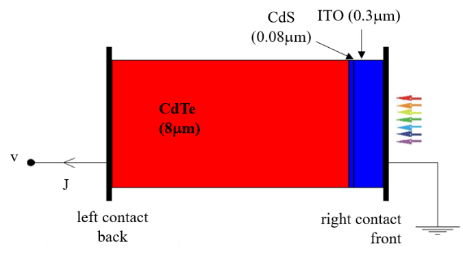
In this study, we used a thin-film solar cell of the following structure ITO/CdS/CdTe/Mo, where Mo plays the role of a back contact, CdTe is the absorbent layer, CdS the buffer layer and ITO the window layer. Figure 1 shows the schematic structure of the solar cell.
Our approach consists in simulating the CdTe-based solar cell with SCAPS (Burgelman et al., 2004; Burgelman et al., 2000; Burgelman et al., 2019) in order to optimize its electrical output characteristics, namely the open-circuit voltage (Voc), the short-circuit current density (Jsc), the Form Factor (FF) and the efficiency (η) as functions of the properties (thickness and gap energy) of the component layers.
Developed in the Department of Electronic and Computer Systems (ELIS), University of Gent in Belgium, under the supervision of Burgelman et al., (2004); Burgelman et al., (2000) and Burgelman et al., (2019), the SCAPS calculation technique is based on the resolution of Poisson and continuity equations for electrons and holes:
$ \dfrac{d^2\varphi}{{dx}^2} = -\dfrac{q}{\varepsilon_0\varepsilon_r}\left(p - n - N_A^ - +N_D^+ + \dfrac{\rho_t}{q}\right) ~~~~~~~~~~~~~~~~~~~~~~~~ (1)$
and,
$ \cases{ \dfrac{1}{q}\dfrac{dJ_x}{dx}=G-R_n \cr\cr -\dfrac{1}{q}\dfrac{dJ_p}{dx}=G-R_p } ~~~~~~~~~~~~~~~~~~~~~~~~~~~~~~~~~~~~~~~~~~~~~~~~~~~~~~~~~~~~~ (2)$
In Eq. (1) and (2), 𝜑 describes electrical potential, q is the unit charge, 𝜀0 and 𝜀𝑟 are the dielectric constants of vacuum and semiconductor, respectively; n and p are electron and hole densities, respectively; N_A and ND+ are the density of ionized donors and acceptors, 𝜌𝑡 the charge density of defects, 𝐽𝑛 and 𝐽𝑝 the electron and hole current density; G is the generation rate and Rn(p) is the recombination loss.
The transportation of carriers is shown by:
$ \cases{ J_n = -qD_n\dfrac{dn}{dx} + q\mu_n\dfrac{d\varphi}{dx} \cr\cr J_p = -qD_p\dfrac{dp}{dx} - q\mu_p\dfrac{d\varphi}{dx} } ~~~~~~~~~~~~~~~~~~~~~~~~~~~~~~~~~~~~~~~~~~~~~~~~~ (3)$
where,$𝜇𝑛(𝑝)$ : The electron/hole mobility
$Dn(p)$ : The diffusion coefficient
The generation rate function is given by:
$ G\left(\lambda,x\right) = \varphi_0(\lambda)e^{-\alpha\left(\lambda\right).x} ~~~~~~~~~~~~~~~~~~~~~~~~~~~~~~~~~~~~~~~~~~~~~~~~~~~~~~~ (4)$
where,$𝜑_0$ : The incident photon flux
$x$ : A depth
$α$ : The absorption coefficient of the active material and $λ$, the absorbed photon wavelength
Cell performance was achieved with SCAPS under standard conditions (a cell temperature of 25°C and radiation of 1000 W/m² with an air mass coefficient of 1.5 (AM1.5)).
Some additional material parameters used in this simulation were selected based on literature values, theory and experiment are placed in Table 1 (Burgelman et al., 2019; Shen et al., 2016).
| Specific parameters | ITO | CdS | CdTe |
|---|---|---|---|
| Relative dielectric permittivity | 9.00 | 10.00 | 10.2 |
| Effective state density in the BC (cm-3) | 2.20 10+18 | 2.20 10+18 | 8.0 10+17 |
| Effective density of states in BV (cm-3) | 1.80 10+19 | 1.80 10+19 | 1.80 10+19 |
| Electrons mobility (cm2/Vs) | 1.0 10+2 | 1.0 10+2 | 3.2 10+2 |
| Holes mobility (cm2/Vs) | 2.5 10+1 | 2.5 10+1 | 4.0 10+1 |
| Donor density ND (cm-3) | 1.0 10+17 | 1.0 10+17 | 0.0 |
| Acceptor density NA (cm-3) | 0.0 | 0.0 | 1.0 10+14 |
| Absorption coefficient (cm-1) | 1.0 10+6 | SCAPS | 1.0 10+5 |
Results And Discussion
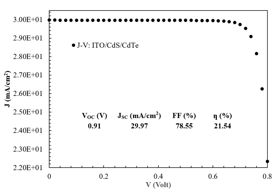
J-V characteristic of the CdTe solar cell: The characteristic J-V curve obtained by the simulation of the ITO/CdS/CdTe/Mo cell to the values in Table 1 shows an efficiency of 21.54% (Fig. 2); which is close to that of practical CdTe solar cells (Gloeckler et al., 2013; Morales-Acevedo, 2006).
This shows that our solar cell model is valid and can be used to make a simulation by studying the effects of different parameters of the material on the cell performances.
The evolution of parameters such as Jsc, Voc, FF and in particular of the efficiency (η) according to the thickness of CdTe, CdS and ITO layers and of the gap energy of the absorbent layer is studied in the following paragraphs.
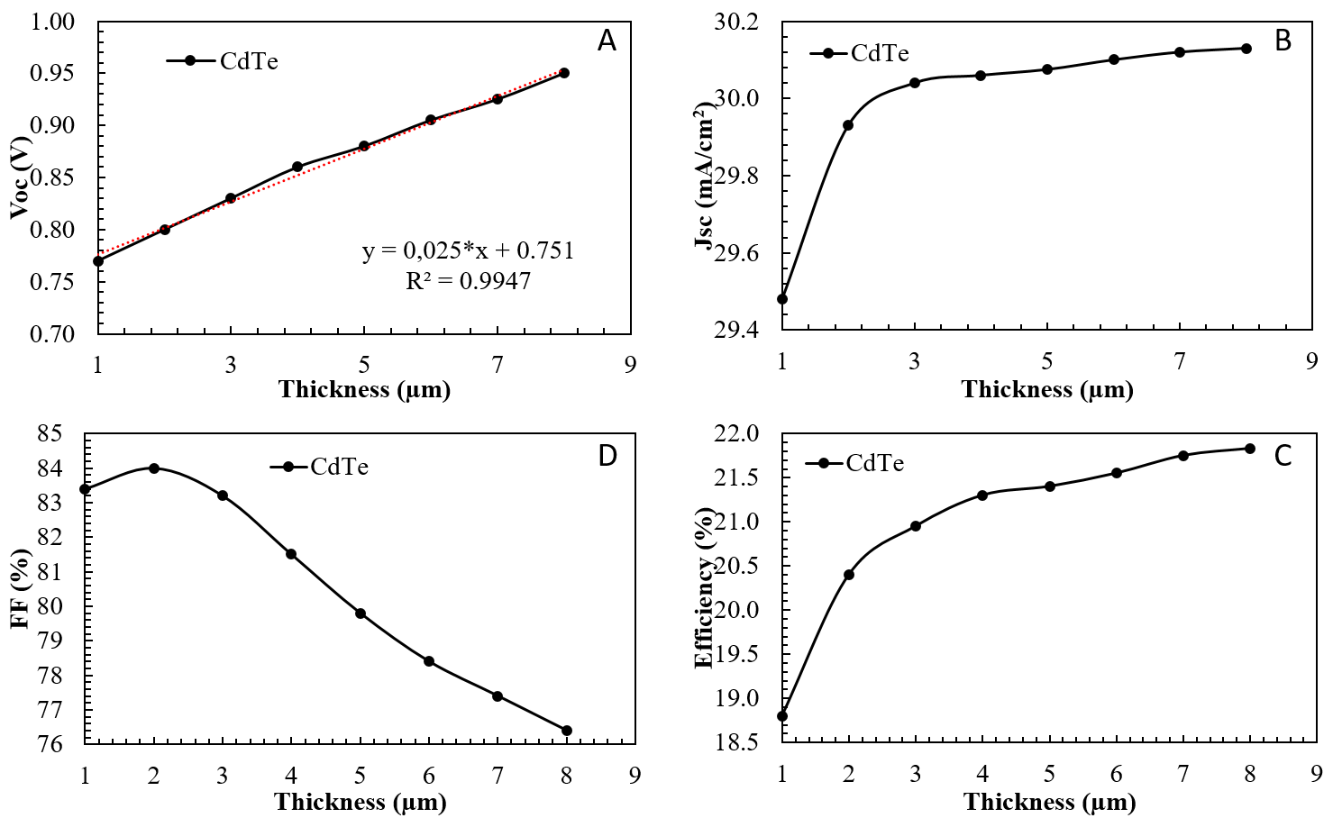
Influence of the thickness of the CdTe layer: The effect of the CdTe absorber thickness (in the range 1-8 µm in steps of 1 µm) on the cell performances like Voc, Jsc, FF and the efficiency is shown in Fig. 3. All the other parameters are kept constant. The increase in the thickness of CdTe leads to an increase of the open-circuit voltage (Fig. 3A), the short-circuit current density (Fig. 3B) and the efficiency of the cell. (Fig. 3D). However, the Form Factor (FF) drops sharply (Fig. 3C). In fact, higher thicknesses generate resistive components which can affect the form factor (Tchognia et al., 2015). Also, if the optical confinement of the cells is not optimized, part of the high energy photons which penetrate deep into the material can be lost, thus reducing the short-circuit current density (Jsc) (Melis and Aynur, 2011).
Theoretically, when the CdTe layer is very thick, the cell performance degrades. Therefore, an optimal thickness of the CdTe layer is necessary to reach the best performance of the solar cell. In our case, the improvement in efficiency could be due to the absorption of photons with high energy, increasing the number of generated electron-hole pairs.
In addition, the efficiency of the cell varies slightly between 4 and 6 μm: for this reason, it is not necessary to produce solar cells with a very thick CdTe layer, allowing to establish a compromise between efficiency and cost.
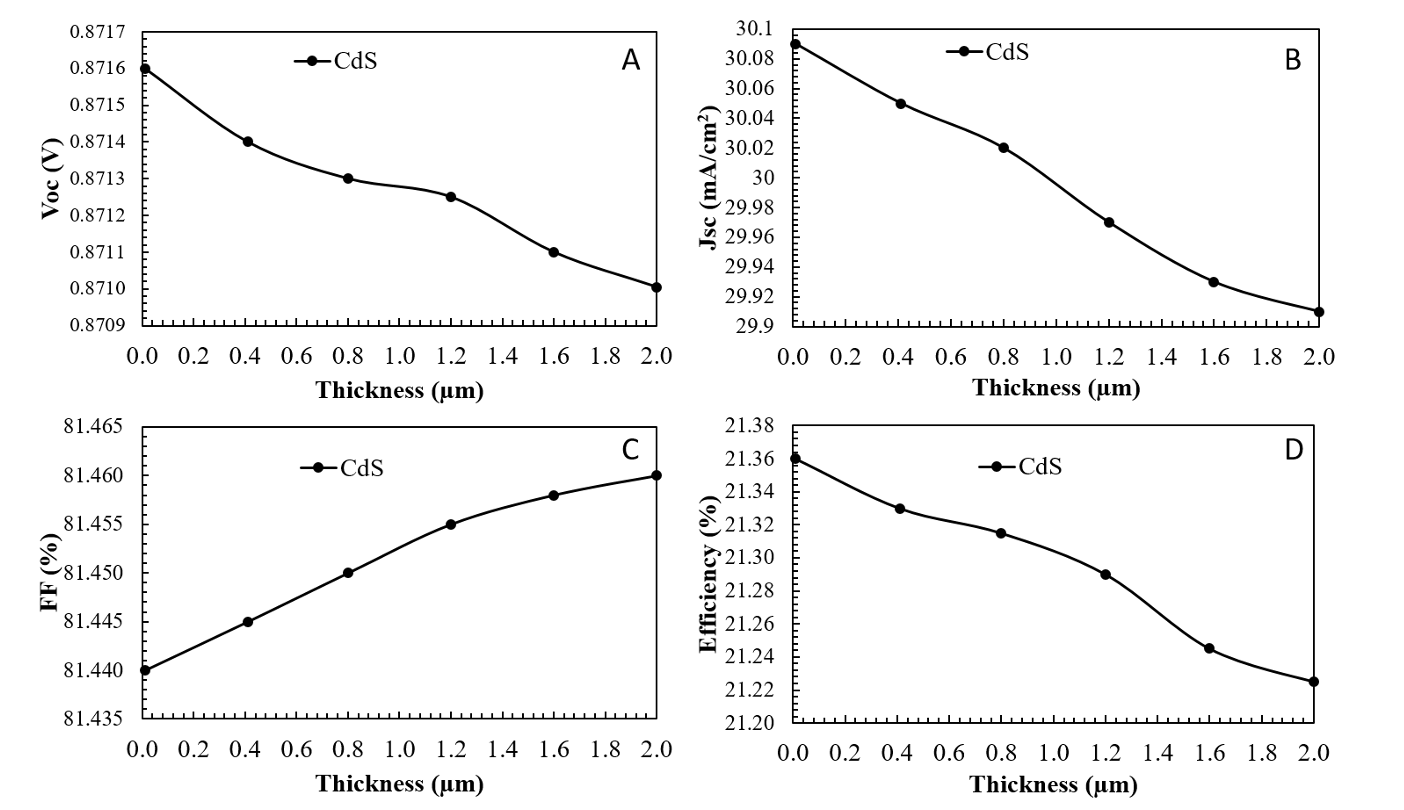
Influence of CdS layer thickness: The increase in the CdS layer between 0.01 and 2 µm in steps of 0.4 leads to an increase in the form factor (Fig. 4C). On the other hand, the open circuit voltage (Fig. 4A), the density of the short-circuit current (Fig. 4B) and the efficiency (Fig. 4D) of the cell decrease.
The buffer layer remains decisive in the protection between the anti-reflective layer and the active layer. CdS film (Eg of 2.4 eV) allow the absorption to occur for short wavelengths. Indeed, a CdS film with a thickness of 0.1 µm can absorb up to 63% of the incidental light with energy values higher than its gap energy (Moualkia et al., 2009). This may be an explanation for the decrease observed on the efficiency for the thicker layers.
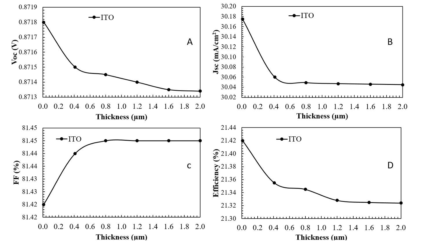
Influence of ITO thickness: The performance of our solar cell model also depends on the thickness of the ITO layer, between 0.04 and 2 µm (Fig. 5). The open-circuit voltage (Fig. 5A), the short-circuit current (Fig. 5B) and the efficiency (Fig. 5C) all decrease with increasing thickness of ITO, whereas the form factor increases (Fig. 5D).
In fact, a better structure should have a thin window layer (Khelifi and Belghachi, 2004). Through this study, we have noticed that the thicknesses of each component layer of the solar cell have a particular influence on the characteristic photovoltaic quantities. Other characteristics of the material also have an influence on the solar performance of a cell.
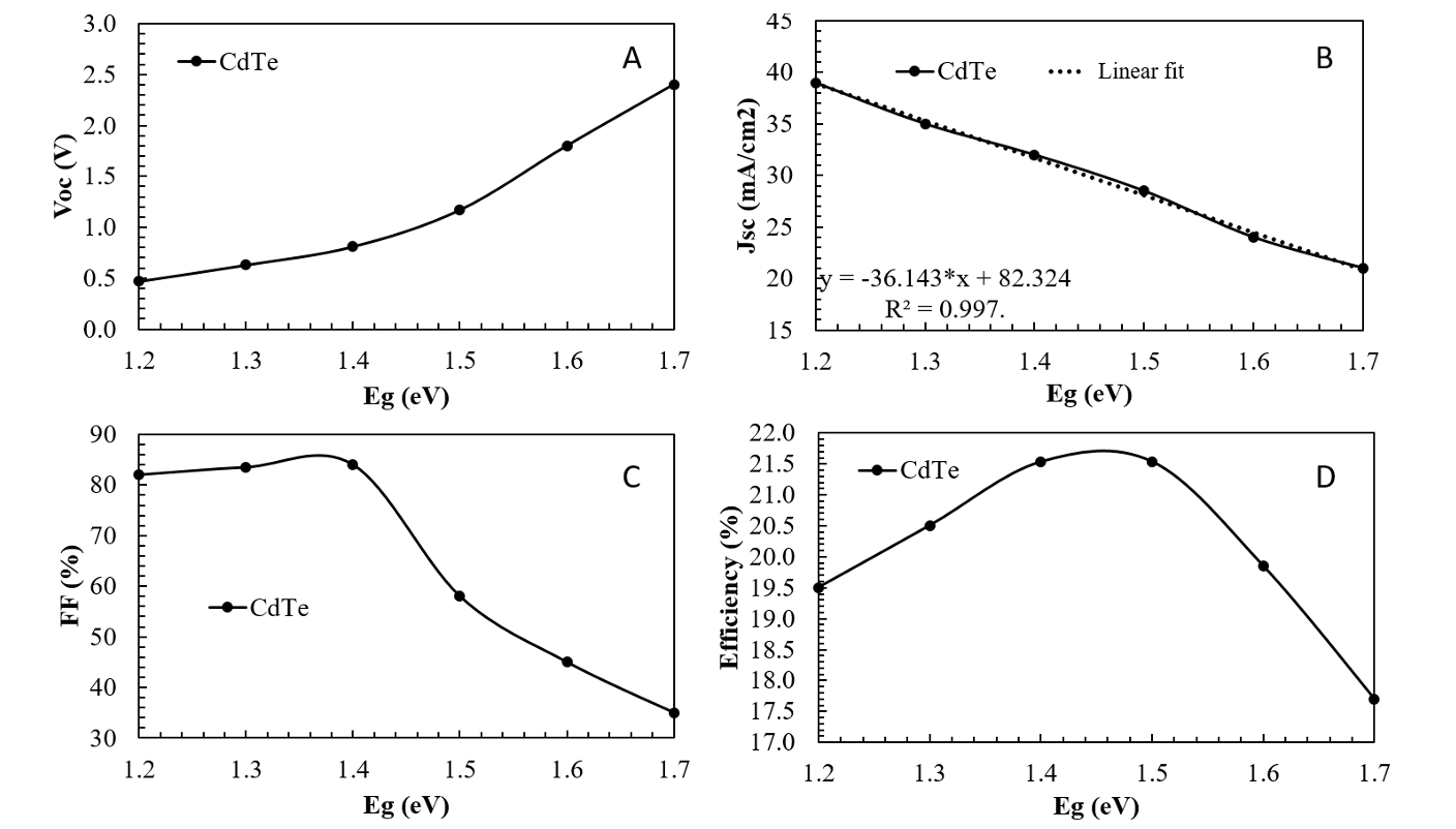
CdTe energy gap effect: We also evaluated the impact of CdTe gap energy on photovoltaic performance with our model (Fig. 6). Maximum efficiency is observed between 1.4 and 1.5 eV. On the other hand, outside this interval, the efficiency is greatly reduced (Fig. 6D). This observation is similar to that made by Benmir and Aida (2013) on a CIGS cell, hence the need to optimize the layer gap.
The Voc (Fig. 6A) of the cell increases when the gap increases. While the Jsc decreases linearly (y = -36.147 * x + 82.824 with R2 = 0.9974) from 1.2 to 1.7 eV (Fig. 6A). The Form Factor increases slightly until the gap of 1.41 eV then decreases rapidly (Fig. 6C).
These results are in agreement with the literature. The widening of the optical gap of the CdTe absorber layer reduces the form factor and the density of the photocurrent while the open circuit voltage increases (Belghachi and Limam 2017; Shoewu et al., 2016). These behaviors may result from the fact that wide gap absorbers do not absorb long wavelength photons. We can therefore observe a small quantity of electron-hole pairs generated andthusasmall quantity of the free carriers collectedwhich reduces thevalue of Jsc (Tchognia et al., 2015). The decrease in maximum efficiency 21.82% which corresponds to 1.47 eV is due to the decrease in Jsc and FF because the open-circuit voltage increases after this value (Fig. 6D).
The optimal performance of the ITO/CdS/CdTe/Mo solar cell: The CdTe thin-film solar cell in the ITO/CdS/CdTe/Mo structure has an optimal conversion efficiency of 22% (Table 2), taking into account the energy gap value of CdTe and the optimized thicknesses of ITO and CdS. Thus, the results obtained show that each characteristic of each layer has a very important role vis-à-vis the device under study and particularly, can allow the improvement of the PV conversion efficiency. Indeed, an increase in the thickness of the transparent ITO conductive oxide layer and of the CdS buffer layer of the cell reduces the PV efficiency. However, the electrical performance increases with the thickness of the CdTe absorber layer.
For the influence of the gap energy of CdTe, it can generate a reduction of the density of the photocurrent but can increase the open circuit voltage in certain interval being able to reach efficiencies of 22.00% with 1.015V open-circuit voltage and a court-circuit current density of 30.09 mA/cm2 (Table 2).
The CdTe-based thin-film solar cell is a good candidate for the manufacture of photovoltaic solar modules.
| Voc | Jsc (mA/cm2) | FF (%) | ɳ (%) |
|---|---|---|---|
| 1.01 | 30.09 | 72.00 | 22.00 |
Conclusion
In this study, we were able to establish, by simulation with SCAPS, that the thickness and optical gap of each layer of the ITO/CdS/CdTe/Mo structure impacts the performance of this thin layer solar cell (Voc, Jsc, FF and η). Indeed, we achieved a maximum conversion yield of 22.00%.
It appears from the simulations that it is necessary to control the properties of the component layers of the structure of the solar cell in order to have more efficient and more suitable photovoltaic solar modules.
Finally, great hopes lie in the use of thin-film photovoltaic modules based on CdTe to achieve competitive costs for the production of electricity with high efficiency.
Acknowledgment
All authors thank the physics department of UFR SATIC at AliouneDiop University, Bambey (Senegal) for the collaboration through the Interuniversity Master of Renewable Energy (MIER) and Pr. Marc Burgelmanet al. from the University of Gent, Belgium for the provision of the SCAPS thin film solar cell simulation program.
Conflict of Interest
We declare that we do not have any commercial or associative interest that represents a conflict of interest in connection with the work submitted. The results are not related to previous findings.
Author Details
1Département de Physique, UFR SATIC, UniversitéAliouneDiop de Bambey Senegal
2Laboratoire de Physique de la MatièreCondensée (LPMC), Université de Picardie Jules Verne, Chemin du Thil - CS 52501 - 80025 AmiensCedex-1
3Laboratoire de Chimie Physique Organique et d'AnalysesEnvironnementales (LCPOAE), UniversitéCheikh Anta Diop, BP 5005 Dakar‐Fann, Dakar
References
Benmir, A. and M.S. Aida, 2013. Analytical modeling and simulation of CIGS solar cells. Energy Proc., 36: 618-627.
Burgelman, M., P. Nollet and S. Degrave, 2000. Modelling polycrystalline semiconductor solar cells. Thin Solid Films, 361-362: 527-532.
Burgelman, M., J. Verschraegen, S. Degrave and P. Nollet, 2004. Modeling thin‐film PV devices. Prog. Photovoltaics: Res. Appl., 12: 143-153.
Burgelman, M., K. Decock, A. Niemegeers, J. Verschraegen and S. Degrave, 2019. SCAPS Manual.
Gloeckler, M., I. Sankin and Z. Zhao, 2013. CdTe solar cells at the threshold to 20% efficiency. IEEE J. Photovoltaics, 3: 1389-1393.
Green, M.A., K. Emery, Y. Hishikawa, W. Warta and E.D. Dunlop, 2015. Solar cell efficiency tables (version 51). Prog. Photovoltaic: Res. Appl., 26: 3-12.
Khelifi, S. and A. Belghachi, 2004. Le Rôle de la Couche Fenêtre dans les Performances d'une Cellule Solaire GaAs. Rev. Energ. Ren., 7: 13-21.
Lincot, D., 2007. La conversion photovoltaïque de l'énergie solaire. Palais de la découverte, 344-345: 47-65.
Luan, W., C. Zhang, L. Luo, B. Yuan, L. Jin and Y.S. Kim, 2017. Enhancement of the photoelectric performance in inverted bulk heterojunction solid solar cell with inorganic nanocrystals. Appl. Energ., 185: 2217-2223.
Melis, B.A. and E. Aynur, 2011. Optimization of a-Si:H/c-Si heterojunction solar cells by numerical simulation. Energ. Proc., 10: 101-105.
Miles, R.W., G. Zoppi and I. Forbes, 2007. Inorganic photovoltaic cells. Mater. Today, 10(11): 20-27.
Mitchell, K., A.L. Fahrenbruch and R.H. Bube, 1977. Photovoltaic determination of optical‐absorption coefficient in CdTe. J. Appl. Phys., 48: 829..
Morales-Acevedo, A., 2006. Thin film CdS/CdTe solar cells: Research perspectives. Sol. Energy, 80(6): 675-681.
Moualkia, H., S. Hariech and M.S. Aida, 2009. Structural and optical properties of CdS thin films grown by chemical bath deposition. Thin Solid Films, 518(4): 1259-1262.
Parida, B., S. Iniyan and R. Goic, 2015. A review of solar photovoltaic technologies. Renew. Sust. Energ. Rev., 15(3): 1625-1636.
Paudel, N.R. and Y. Yan, 2015. Fabrication and characterization of high-efficiency CdTe-based thin-film solar cells on commercial SnO2:F-coated soda-lime glass substrates. Thin Solid Films, 549: 30-35.
Saga, T., 2010. Advances in crystalline silicon solar cell technology for industrial mass production. NPG Asia Mater., 2: 96-102.
Shen, K., Q. Li, D. Wang, R. Yang, Y. Deng, M.J. Jeng and D. Wang, 2016. CdTe solar cell performance under low-intensity light irradiance. Sol. Energ. Mat. Sol. C., 144: 472-480.
Shoewu, O., G. Anuforonini and O. Duduyemi, 2016. Simulation of the performance of CdTe/CdS/ZnO multi- junction thin film solar cell. Rev. Inform. Eng. Appl., 3(1): 1-10.
Tchognia, J.H.N., B. Hartiti, J.M. Ndjaka, A. Ridah and P. Thevenin, 2015. Performances des cellules solaires à base de Cu2ZnSnS4 (CZTS): Une analyse par simulations numériques via le simulateur SCAPS. Afr. Sci., 11(4): 16-23.
Rights and permissions
Open Access: This article is licensed under a Creative Commons Attribution 4.0 International License, which permits use, sharing, adaptation, distribution and reproduction in any medium or format, as long as you give appropriate credit to the original author(s) and the source, provide a link to the Creative Commons license, and indicate if changes were made. The images or other third-party material in this article are included in the article’s Creative Commons license, unless indicated otherwise in a credit line to the material. If material is not included in the article’s Creative Commons license and your intended use is not permitted by statutory regulation or exceeds the permitted use, you will need to obtain permission directly from the copyright holder. To view a copy of this license, visit http://creativecommons.org/licenses/by/4.0/
Cite this Article
El HadjiNdiougaNdiaye, Serigne MassambaSeck, Modou Fall and Stéphane Charvet, 2020. Optimization of the Electrical Characteristics of Cadmium Telluride Based Thin Layer Solar Cell According to Thickness and Gap Energy. Research Journal of Applied Sciences, Engineering and Technology 17: 129-135 http://doi.org/10.19026/rjaset.17.5821
Received
Accepted
Published
March 13, 2020
April 30, 2020
August 25, 2020
DOI: http://doi.org/10.19026/rjaset.17.5821
Sections
Abstract
Keywords
Introduction
Materials And Methods
Results And Discussion
J-V characteristic of the CdTe solar cell
Influence of the thickness of the CdTe layer
Influence of CdS layer thickness
Influence of ITO thickness
CdTe energy gap effect
The optimal performance of the ITO/CdS/CdTe/Mo solar cell
Conclusion
Acknowledgement
Conflict of Interest
Author Details
References
Rights And Permissions
Cite This Article